When designing a PCB, engineers often spend a lot of time thinking about signal traces and power traces.
However, there is another path that is equally important:
The return current path.
A signal does not simply travel from one component to another and disappear.
Current must complete a loop.
For many PCB designs, a properly designed ground plane provides a low-impedance return path and helps control signal integrity and electromagnetic interference (EMI). TI and Analog Devices both emphasize the importance of maintaining continuous reference/ground planes and controlling return-current paths.
This is why PCB grounding should be considered during component placement and routing—not as an afterthought.
1. What Is a PCB Ground Plane?
A ground plane is a large area of copper used as a common electrical reference and return path.
On a two-layer PCB, a common arrangement is:

Instead of routing a separate narrow ground trace to every component, the PCB can use a large copper area.
This can reduce the impedance of the return path and simplify PCB routing.
2. Why Is Ground Important?
Consider a simple circuit:

The signal current must return to the source.
Therefore, the actual electrical loop is:
Source → Signal → Load → Ground/Return → Source
If the return path has high impedance, the voltage at different ground locations may not be exactly the same.
This becomes increasingly important when:
- Current changes rapidly
- Digital signals switch quickly
- Switching regulators are used
- Analog measurements are sensitive
- Communication signals are involved
Analog Devices explains that return current follows the path of least impedance and that, at higher frequencies, it tends to remain close to the associated signal path because that minimizes loop area.
3. Ground Is Not Always “Zero Volts”
This is an important engineering concept.
We often draw:
GND = 0 Von a schematic.
But on a real PCB, copper has:
- Resistance
- Inductance
- Parasitic capacitance
Therefore, when current flows through the ground structure, there can be a voltage difference between two physical points.
A simplified relationship is:V=I×RV=I\times R
For rapidly changing currents, inductance also becomes important:V=LdidtV=L\frac{di}{dt}
This means that even a small amount of inductance can produce significant transient voltage when current changes rapidly.
Analog Devices specifically notes that increasing return-path inductance can increase voltage noise according to V=L(di/dt)V=L(di/dt).
4. Ground Plane vs Ground Trace
Consider two approaches.
Ground trace

The ground return is a relatively narrow conductor.
Ground plane

The second arrangement can provide a much broader return-current path.
For many digital and mixed-signal PCBs, a continuous ground plane is therefore very useful.
However, larger copper does not automatically solve every grounding problem.
The location of components and the actual current paths still matter.
5. Return Current Is the Key
This is one of the most important concepts in PCB design.
Suppose we have:

The signal current needs a return path.
With a continuous ground plane:
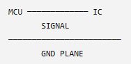
At higher frequencies, much of the return current tends to flow in the ground plane close to the signal trace.
This reduces the loop area.
A smaller loop generally helps reduce parasitic inductance and unwanted electromagnetic coupling. Analog Devices describes this behavior in its grounding application notes.
6. Why Ground Plane Continuity Matters
Now imagine that someone cuts the ground plane underneath a signal trace.

The return current cannot simply travel directly underneath the signal.
It must go around the opening.

This increases the return-current loop area.
It can also increase inductance and create unwanted coupling.
TI’s PCB design guidance specifically warns that discontinuities in a reference plane can force return currents around obstacles, increasing crosstalk, impedance discontinuities, and EMI.
7. Ground Plane and High-Speed Signals
The faster a signal changes, the more important its return path becomes.
For example:
Relatively slow signal
A simple control signal may be less sensitive to small PCB layout changes.
Fast digital signal
A fast clock or high-edge-rate digital signal can behave much more like a transmission-line problem.
Important factors include:
- Trace geometry
- Dielectric thickness
- Ground-plane distance
- Return-current path
- Via transitions
- Impedance
- Trace length
Therefore, the question is not simply:
“What is the signal frequency?”
The edge rate and physical dimensions of the interconnect also matter.
8. Two-Layer PCB Ground Design
For a simple two-layer PCB, a practical starting point is:
Top
- Components
- Main signal routing
- Some power routing
Bottom
- Mostly continuous GND copper
For example:
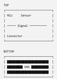
This is not a universal rule, but it is a useful starting architecture for many relatively simple boards.
9. Don’t Create Unnecessary Ground Islands
One common mistake is creating isolated copper areas that look like ground but aren’t well connected.
For example:

If these regions are poorly connected, current may be forced to take longer paths.
TI recommends avoiding ground-plane islands and making sure return currents are not forced around unnecessary obstacles.
A ground plane should be electrically useful, not simply visually large.
10. Ground Vias
When a signal changes PCB layers, the return path may also need a low-impedance transition.
For example:

Ground vias can be used to connect ground copper between PCB layers.
For high-speed designs, placing an appropriate ground via near a signal via can help maintain a more controlled return path.
The exact arrangement depends on the stackup, signal type, geometry, and design requirements.
11. Ground Plane and Decoupling Capacitors
This connects directly to Part 3.
A decoupling capacitor should have a short path between:
Power pin → capacitor → ground
For example:

The capacitor’s ground connection should also be low impedance.
Analog Devices recommends placing power-supply bypass capacitors close to IC power pins and connecting them to the ground plane with a low-inductance path.
12. Ground Plane and MCU Stability
This is particularly relevant to controller PCB design.
A simplified system is:

If the MCU power supply or ground reference becomes noisy, you may see:
- Unexpected reset
- Communication errors
- ADC errors
- Flash programming problems
- Startup problems
- Intermittent operation
This doesn’t mean every MCU failure is caused by the ground plane.
The power supply, reset circuit, firmware, clock, EMI, and component selection must also be investigated.
But the PCB return path is an important part of the system.
13. Analog Ground and Digital Ground
This subject often causes confusion.
A common assumption is:
“Always separate analog ground and digital ground.”
That is not universally correct.
For many mixed-signal systems, Analog Devices recommends a solid single ground plane when the system architecture permits it. Splitting the ground plane can actually increase return-path inductance and noise if done without a clear reason.
The better approach is:
Understand where the currents flow.
Partition the circuits physically when possible:

Then manage the return paths appropriately.
14. When Ground Separation Can Be Useful
There are designs where separate analog and power/digital ground regions can be appropriate.
For example:
- High-current switching circuits
- Precision analog systems
- ADC/DAC systems
- Sensitive measurement circuits
- Specialized power converters
But the separation must be based on the actual current paths.
Analog Devices’ guidance for some mixed-signal and converter applications uses separate regions and carefully controlled connections between them.
Therefore:
Don’t split the ground plane simply because someone told you that analog and digital ground must always be separated.
Instead ask:
Where does the return current flow?
That is the more important engineering question.
15. Switching Power Supply Ground
This is particularly important for the PCB power supply discussed in Part 3.
A switching regulator can produce high-frequency current loops.
Simplified:
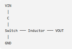
The high-current switching loop should be kept physically small.
The power components and their ground returns should be arranged according to the regulator manufacturer’s recommended layout.
Analog Devices’ switching-regulator guidance distinguishes high-current power ground from quieter analog ground regions in some converter architectures.
16. RS-485 and Ground Plane
Grounding is also important in industrial communication.
For an RS-485 PCB:
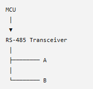
The differential A/B pair carries the communication signal, but the complete system still needs an appropriate reference and grounding strategy.
The PCB layout should consider:
- A/B routing
- Differential geometry
- Termination
- Bias network
- Connector
- Ground/reference
- Shield
- Isolation, if required
This connects directly to the PowerTechGuide article:
Industrial Communication Problems: Cable Connection, Impedance Matching, and Termination Resistors
17. Ground Plane and EMI
A properly designed ground plane can help reduce unwanted electromagnetic coupling by providing a close return path.
The basic idea is:
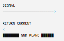
The closer the return path is to the signal path, the smaller the loop area can become.
Analog Devices notes that keeping the return path close to the signal conductor helps reduce inductance and electromagnetic fields.
However, a ground plane alone does not guarantee EMI compliance.
Component placement, cable routing, shielding, filtering, enclosure design, switching loops, and common-mode currents can all matter.
18. Real-World Engineering Experience
This is another place where your own engineering experience can strengthen the PowerTechGuide article.
Power Reset Problem
During the development of a main controller unit, I experienced an intermittent startup problem under unstable power-input conditions.
The power reset signal was not stable enough during startup, and the controller occasionally failed to start.
I modified the power-reset circuit and changed the boot-control signals so that the relevant signals had a defined logic state during power-up.
This experience reinforced an important engineering principle: reliable digital operation requires stable power, a reliable ground reference, a properly designed reset circuit, and clearly defined control signals.
This is a strong example because it connects:
Power Supply → Ground → Reset → MCU → Boot → System Startup
19. How to Troubleshoot a Grounding Problem
When a PCB has intermittent problems, don’t immediately replace the IC.
Use a systematic approach.
Step 1 — Check power
Measure:
- VIN
- VCC
- regulator output
Step 2 — Check ground
Measure voltage between important ground points.
Step 3 — Check current
Look for unexpected current changes.
Step 4 — Use an oscilloscope
Check:
- VCC ripple
- Ground noise
- Reset signal
- Clock
- Communication signals
Step 5 — Check return paths
Ask:
Where does the current actually return?
Step 6 — Inspect PCB layout
Look for:
- Ground-plane gaps
- Long return paths
- Narrow ground traces
- Poor via placement
- Switching-current loops
- Noisy circuits next to sensitive circuits
20. A Practical Ground Plane Checklist
Before manufacturing a PCB:
Ground Plane
☐ Is there a continuous ground reference where appropriate?
☐ Are unnecessary plane gaps avoided?
☐ Are ground islands properly connected?
☐ Are high-current return paths controlled?
Signal Integrity
☐ Does the signal have a reasonable return path?
☐ Are high-speed signals routed over a continuous reference plane?
☐ Are layer transitions supported by an appropriate return path?
Power
☐ Are regulator ground paths short?
☐ Are decoupling capacitors close to IC power pins?
☐ Are switching-current loops minimized?
Analog
☐ Are sensitive analog circuits physically separated from noisy circuits?
☐ Are analog return currents prevented from sharing noisy paths where appropriate?
Communication
☐ Is the RS-485/CAN return/reference strategy appropriate?
☐ Are connector and shield connections intentionally designed?
Conclusion
A PCB ground plane is much more than a large area of copper.
It is part of the electrical system.
The key concept is:
Every signal has a return path.
A good PCB designer therefore doesn’t only ask:
“Where does the signal go?”
The designer also asks:
“Where does the return current go?”
That question becomes increasingly important as signal edge rates increase, switching currents become larger, and analog measurements become more sensitive.
For many PCB designs, a continuous ground plane provides an effective low-impedance return path. But ground design must ultimately be based on the actual circuit architecture and current flow—not on a blanket rule to either split or not split the ground plane.
Good PCB design is not simply about connecting components. It is about controlling current, voltage, return paths, noise, and signal integrity.
3 Responses