- Introduction
High-speed LED strobe controllers are widely used in machine vision, industrial inspection, optical measurement, and automated manufacturing systems.
In the original design, I developed a high-speed LED strobe controller using an NXP MPC5744P microcontroller, Lattice CPLD, TFT display, and high-speed line-driver switching device.
As system requirements increased, the controller was upgraded from the MPC5744P to the MPC5748G.
The main objectives of the version upgrade were:
- Upgrade the MCU from MPC5744P to MPC5748G
- Add SIO functionality
- Add additional LED control inputs
- Expand the available clock frequency range
- Expand the LED strobe duty-cycle range
- Improve system flexibility and external system integration
This article describes the architecture, the reason for the MCU upgrade, and the engineering considerations involved in expanding the system.
Note: Customer-specific information, proprietary circuit values, firmware source code, and confidential design details are omitted.
1. Original MPC5744P-Based LED Strobe Controller
The original controller was based on the following architecture:
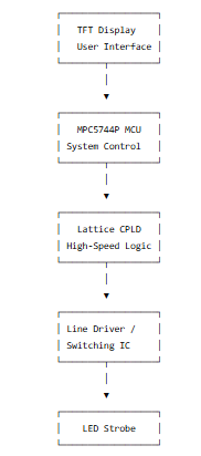
The MPC5744P handled system-level functions while the CPLD handled timing-critical digital logic.
This architecture provided a clear separation between:
MCU = System Control
CPLD = High-Speed Deterministic Logic
2. Why Upgrade from MPC5744P to MPC5748G?
The original MPC5744P design successfully provided the required LED strobe functions.
However, the next-generation controller required additional capabilities.
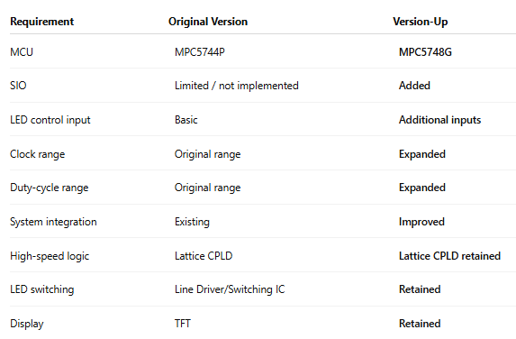
The important point is that the upgrade was driven by system requirements, rather than simply replacing the MCU with a newer device.
3. MPC5744P vs. MPC5748G
The two MCU generations provide different levels of system capability and peripheral resources.
For this LED strobe controller, the most important comparison is not simply CPU performance.
The important engineering factors are:
- Available I/O
- Peripheral resources
- Communication interfaces
- Timer capabilities
- ADC resources
- Memory resources
- Processing capability
- Package and pin availability
- System integration requirements
Engineering Comparison
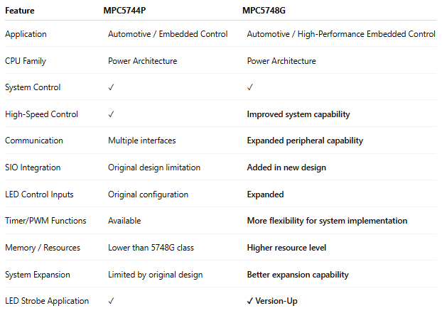
Exact peripheral counts, memory sizes, clock limits, and pin assignments should be taken from the specific NXP device datasheets and the exact package selected for the project.
The important design decision was that the MPC5748G provided a better platform for the expanded system requirements.
4. What Changed in the Version-Up?
The version upgrade can be summarized as:
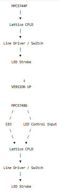
The fundamental architecture remained the same, but the system interface and operating range were expanded.
5. SIO Function Added
One of the major additions in the MPC5748G version was SIO functionality.
SIO provides an additional interface for communication or control between the LED strobe controller and an external system.
A simplified signal flow is:
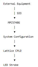
This makes the controller easier to integrate with external industrial equipment and machine-vision systems.
This is especially useful when the LED must be synchronized with a camera or machine trigger.
6. Additional LED Control Inputs
The upgraded version also added additional LED control input signals.
This allows an external machine or inspection system to control the LED strobe.
External Trigger
       │
       ▼
LED Control Input
       │
       ▼
   MPC5748G
       │
       ▼
   Lattice CPLD
       │
       ▼
Line Driver
       │
       ▼
 LED Strobe
This is especially useful when the LED must be synchronized with a camera or machine trigger.
7. Expanded Clock Frequency Range
Another important objective was to increase the available clock frequency range.
The relationship between clock frequency and period is:
T = 1/f
where:
- T = clock period
- f = clock frequency
Increasing the available clock frequency can provide finer timing resolution.
Higher Clock Frequency
          │
          ▼
Shorter Clock Period
          │
          ▼
Higher Timing Resolution
          │
          ▼
More Flexible LED Strobe Control
This was one of the reasons the MPC5748G-based architecture was selected for the version-up design.
8. Expanded Duty-Cycle Range
The upgraded controller also expanded the usable LED strobe duty-cycle range.
Duty cycle is:
Duty(%) = T_ON / T_PERIOD x 100
For example:
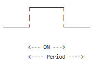
A wider duty-cycle range allows the LED strobe to be configured for different:
- Camera exposure times
- LED power levels
- Object speeds
- Inspection conditions
- Trigger configurations
- Machine-vision applications
9. Why Keep the Lattice CPLD?
Even though the MCU was upgraded from MPC5744P to MPC5748G, the Lattice CPLD remained an important part of the design.
The reason is that MCU software and high-speed deterministic timing have different requirements.
MPC5748G
The MCU handles:
- System control
- SIO
- LED control inputs
- TFT interface
- Configuration
- Communication
- Monitoring
- Error handling
- Parameter management
Lattice CPLD
The CPLD handles:
- High-speed timing
- Trigger processing
- Clock generation
- Pulse generation
- Duty-cycle control
- Deterministic digital logic
Therefore:
The MPC5748G controls the system, while the CPLD handles time-critical digital logic.
This architecture provides both flexibility and deterministic timing.
10. High-Speed LED Switching
The CPLD output drives a high-speed line-driver or switching stage.
MPC5748G
    │
    ▼
Lattice CPLD
    │
    │ High-Speed Logic
    ▼
Line Driver / Switching IC
    │
    │ High-Current Switching
    ▼
LED
The switching device must be evaluated based on:
- Voltage
- Current
- Switching frequency
- Rise time
- Fall time
- Power dissipation
- Thermal characteristics
- Load characteristics
The digital waveform and actual LED current waveform are not necessarily identical.
11. Signal Integrity for the Higher-Speed Version
As the clock and strobe frequency range increases, PCB design becomes increasingly important.
Important considerations include:
- Trace length
- Ground return path
- Impedance
- Crosstalk
- Connector characteristics
- Termination
- Power distribution
- Decoupling
- Ground bounce
- Switching noise
The higher-speed version therefore required attention not only to firmware and MCU selection but also to the complete hardware signal path.
12. Power Integrity
Fast LED switching creates rapidly changing current.
This can produce:
- Supply ripple
- Voltage spikes
- Ground noise
- EMI
- Logic disturbances
- Trigger instability
A simplified system power structure is:
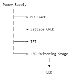
Power integrity must therefore be considered together with signal integrity.
13. Oscilloscope Verification
The actual output waveform should be verified with an oscilloscope.
Important measurements include:
- Clock frequency
- Strobe frequency
- Pulse width
- Duty cycle
- Rise time
- Fall time
- Overshoot
- Undershoot
- Ringing
- Trigger delay
- Supply ripple
A useful measurement path is:
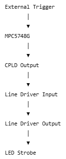
This allows the engineer to determine exactly where timing or waveform degradation occurs.
14. Real-World Engineering Experience
The transition from MPC5744P to MPC5748G was not simply a processor replacement.
The system requirements changed.
The upgraded controller required:
- Additional SIO
- Additional LED control inputs
- Wider clock range
- Wider duty-cycle range
- Greater system flexibility
The existing architecture of MCU + CPLD + high-speed switching stage was therefore maintained while the MCU platform and system interfaces were upgraded.
This is an important lesson in embedded-system development:
A successful version-up should address the actual system limitations while preserving proven portions of the original architecture.
15. Actual Results Table
| Parameter | MPC5744P Version | MPC5748G Version | Result |
|---|---|---|---|
| MCU | MPC5744P | MPC5748G | Upgraded |
| SIO | — / Original | Implemented | Added |
| LED Control Input | Original | Expanded | Added |
| Minimum Clock | 1kHz | 500Hz | 500Hz |
| Maximum Clock | 20kHz | 100kHz | 100kHz |
| Minimum Pulse Width | 4ns | 2ns | 2ns |
| Maximum Pulse Width | 30,000ns | 80,000ns | 80,000ns |
| Strobe Output | Supported | Supported | Verified |
| CPLD | Lattice | Lattice | Retained |
| TFT | Supported | Supported | Retained |
| External Integration | Original | Improved | Improved |
16. Key Lessons from MPC5744P → MPC5748G
Lesson 1 — Identify the original system limitations
The reason for the upgrade should be clearly defined.
In this case:
I/O + SIO + clock range + duty-cycle range + system integration
were the primary requirements.
Lesson 2 — Do not rely on the MCU alone
High-speed timing may still require programmable logic such as a CPLD.
Lesson 3 — Expand the interface capability
SIO and additional LED control inputs make the controller more adaptable to external equipment.
Lesson 4 — Higher speed requires better PCB design
As frequency increases, PCB layout and power integrity become increasingly important.
Lesson 5 — Measure the real hardware
The final design should always be verified using actual waveforms.
Conclusion
The evolution from the MPC5744P-based LED strobe controller to the MPC5748G-based version was a system-level upgrade driven by new functional requirements.
The new version added:
- MPC5748G MCU
- SIO functionality
- Additional LED control inputs
- Expanded clock frequency range
- Expanded duty-cycle range
- Improved system integration
The Lattice CPLD and high-speed line-driver/switching stage were retained because they provided important deterministic timing and high-speed LED switching capabilities.
The final architecture demonstrates how an embedded controller can evolve while maintaining a proven hardware concept:
MPC5748G → System Control
Lattice CPLD → High-Speed Timing
Line Driver/Switching IC → LED Current Switching
TFT → User Interface
SIO + LED Control Input → External System Integration
This MPC5744P-to-MPC5748G version-up is a strong example of practical embedded engineering, where processor selection, programmable logic, high-speed switching, PCB design, power integrity, and system requirements must all be considered together.
One Response