My First PCB Project with Autodesk Fusion: From Schematic to Manufacturing
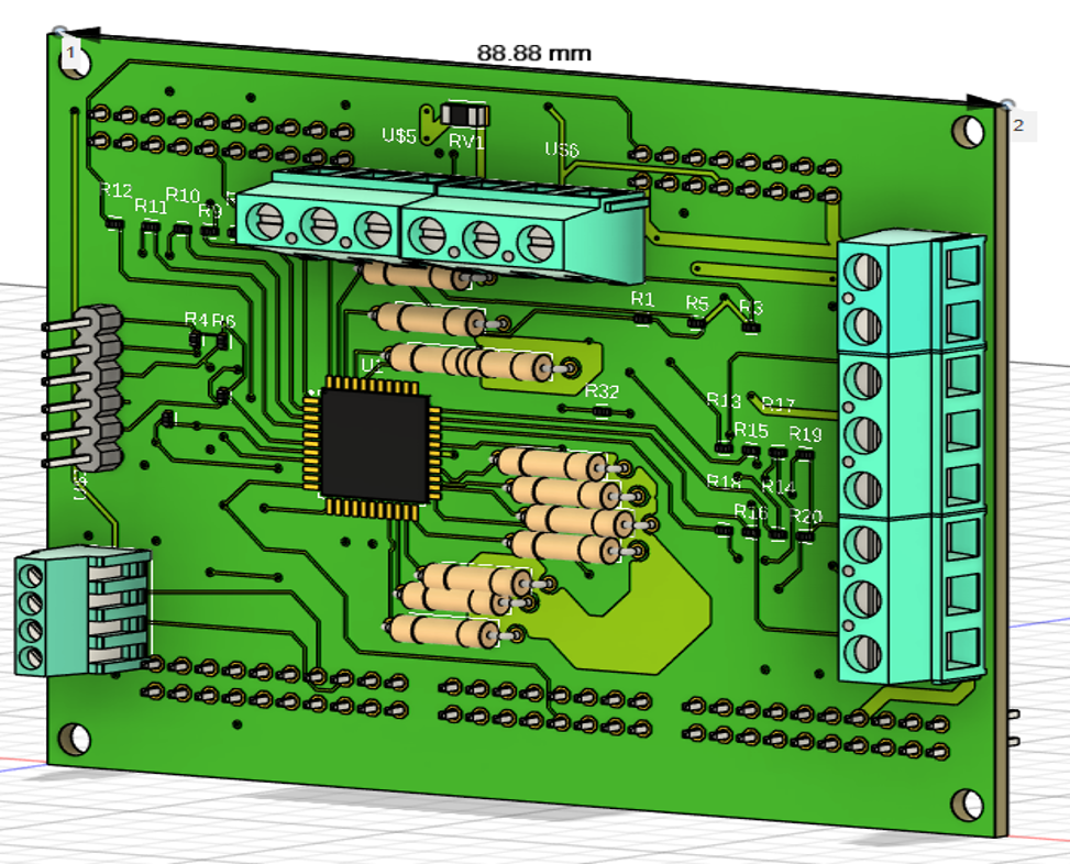
Designing a PCB is much more than drawing copper traces. A complete PCB development process normally includes: Requirements → Schematic → Components → PCB Layout → DRC → 3D Verification → Manufacturing Data → Prototype → Testing Autodesk Fusion Electronics connects the schematic, 2D PCB, and 3D PCB within its electronics design workflow. This article […]
KiCad vs Autodesk Fusion: Which PCB Design Software Is Right for Your Project?

Choosing the right PCB design software can have a major impact on an electronics development project. For a hobby project, you may want software that is free and relatively easy to learn. For a small engineering company, however, PCB layout is only part of the development process. Mechanical design, enclosure dimensions, component placement, manufacturing, and […]
PCB Design Software for Small Businesses and Personal Projects: KiCad, Autodesk Fusion, and More
Designing a PCB is no longer limited to large engineering companies with expensive EDA software. Today, individual engineers, students, makers, startups, and small engineering companies can design professional PCBs using a variety of tools. The important question is: Which PCB design software is appropriate for a small company or an individual engineering project? There is […]